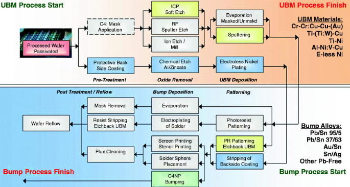
Figure 3 from Under Bump Metallurgy (UBM)-a technology review for


Intermetallic compounds in 3D integrated circuits technology: a

The surface characteristics of under bump metallurgy (UBM) in electroless nickel immersion gold (ENIG) deposition - ScienceDirect

61387 PDFs Review articles in SOLDERING

Materials, Free Full-Text

Figure 3 from Under Bump Metallurgy (UBM)-a technology review for flip chip packaging

Effects of Under Bump Metallurgy (UBM) Materials on the Corrosion of Electroless Nickel Films

SEM images of the cross-sectioned surface of flip-chip eutectic SnPb
Bumps Vs. Hybrid Bonding For Advanced Packaging
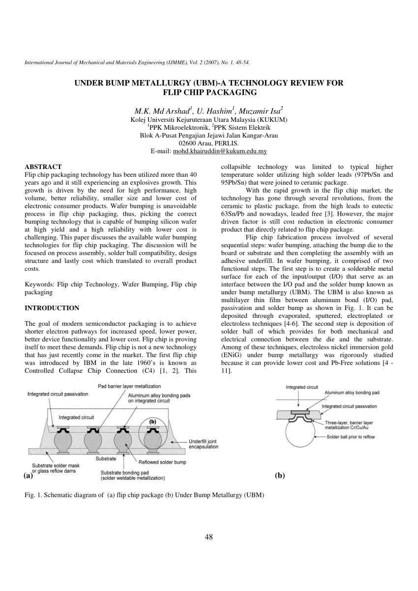
PDF) Under bump metallurgy (UBM) - A technology review for flip chip packaging

PDF) Microstructure Study of High Lead Bump FCBGA Bending Test
Bumping Technologies

61387 PDFs Review articles in SOLDERING
Figure 3 from Under Bump Metallurgy (UBM)-a technology review for flip chip packaging

US9082762B2 - Electromigration-resistant under-bump metallization of nickel-iron alloys for Sn-rich solder bumps in Pb-free flip-clip - Google Patents