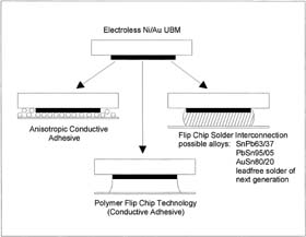
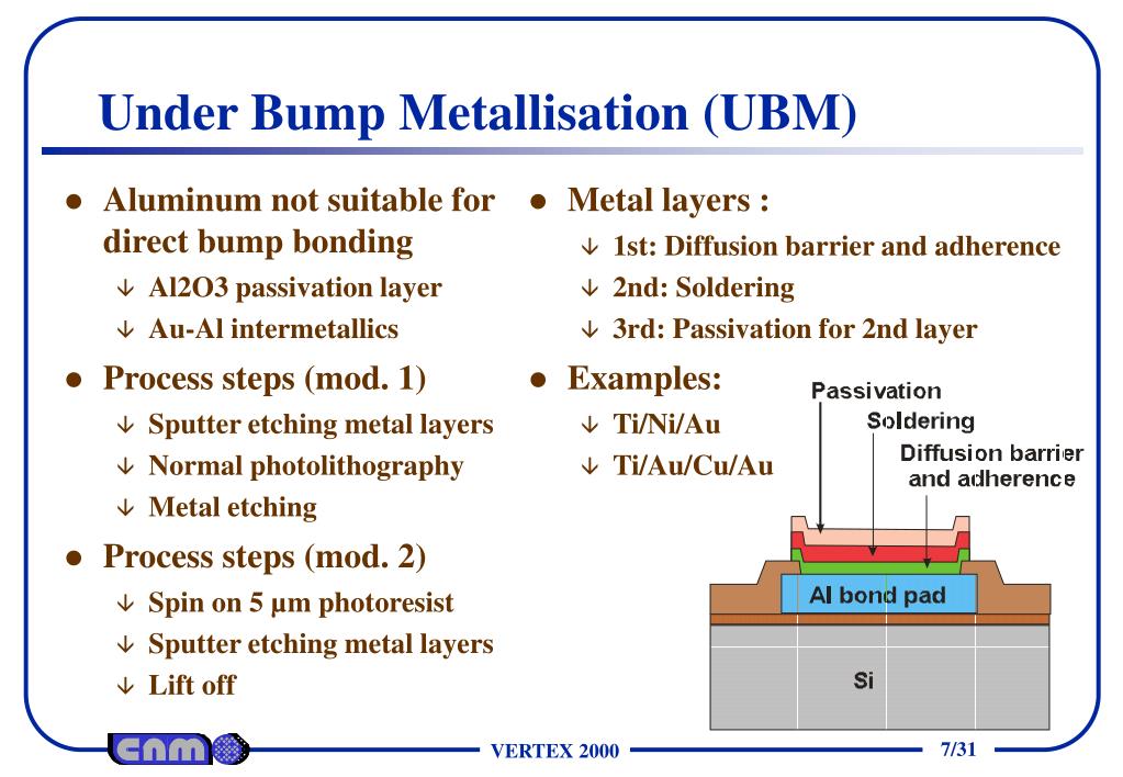
UBM (Under Bump Metallization)
Electromigration-resistant under-bump metallization of nickel-iron alloys for sn-rich solder bumps of pb-free flip-chip applications - Eureka
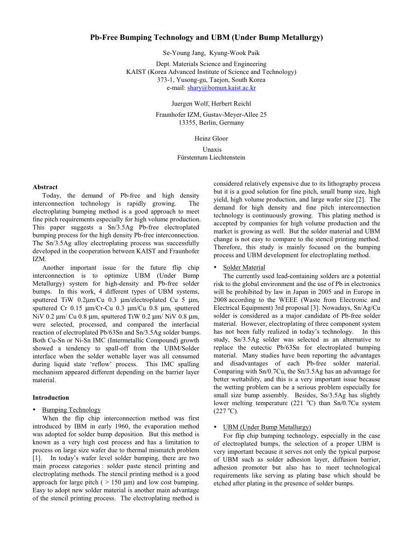
PDF) Pb-free bumping technology and UBM (under bump metallurgy)

Wafer Level Chip Size Package (WLCSP) Guidelines - EEWeb

Eless plating wet bench Vulcanio for efficient UBM (under bump metallization)
The advantages are manifold

SIRIUS-FW
PPT - Summary of Bump Bonding Techniques for Pixel Systems PowerPoint Presentation - ID:245260
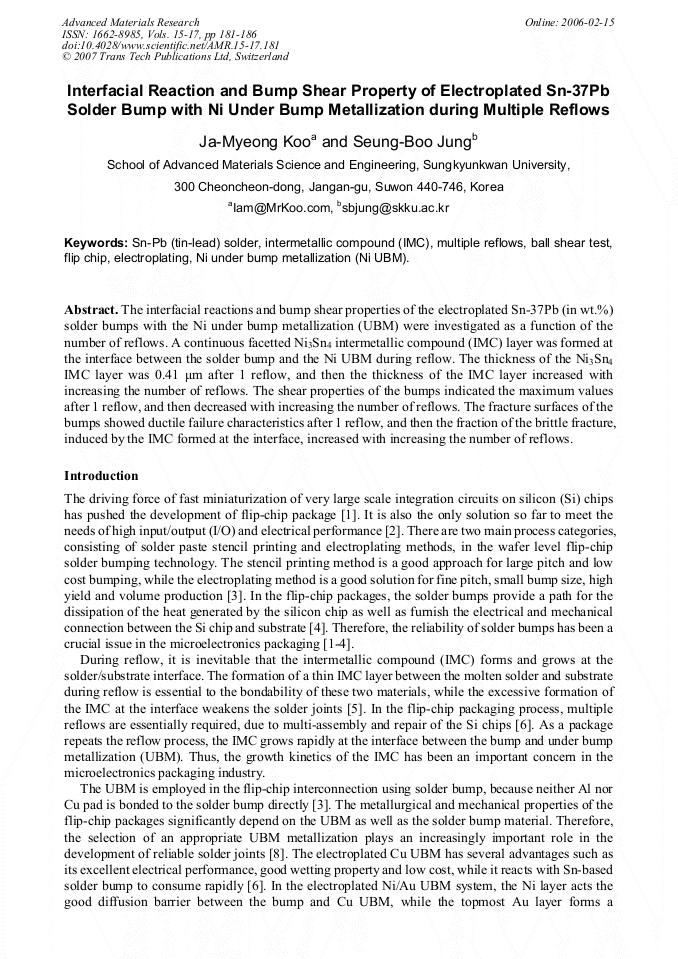
Interfacial Reaction and Bump Shear Property of Electroplated Sn-37Pb Solder Bump with Ni under Bump Metallization during Multiple Reflows

Insights From the Leading Edge: IFTLE 37 Advanced Packaging at Singapores EPTC
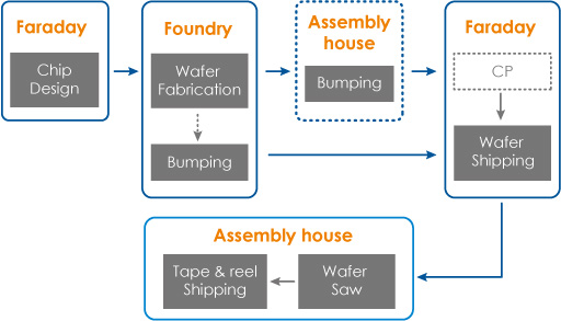
Faraday Technology Corporation-WLCSP Testing & Bumping Process

Interconnection in IC Assembly - ppt video online download

PDF) Pb-free Sn/3.5Ag electroplating bumping process and under bump metallization (UBM)

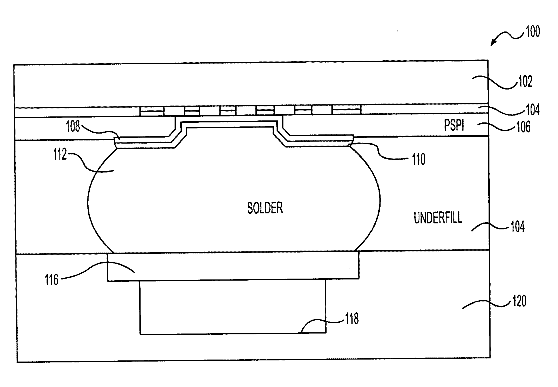
UBM (under bump metallurgy) structure

PDF] CrCu based UBM (under bump metallization) study with electroplated Pb/63Sn solder bumps - interfacial reaction and bump shear strength
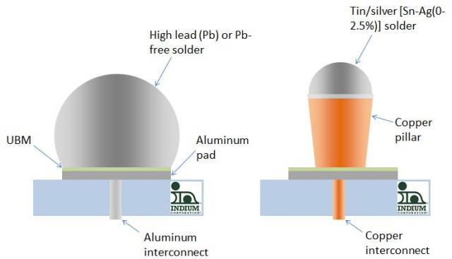
Reflow of Copper Pillar Microbumps, Dr. Andy Mackie, Indium Corporation Blogs, Flux, Solder Flux, Indium Corporation, Solar, Solder Paste, Soldering, Solder