The complete guide to PCB pad :types, size, spacing, repair and

Soldering is one of the most important processes in PCBA processing. On printed circuit boards, electrical connections to all components are made via PCB pads. The PCB pads are a very critical part of the PCB that determines where components are soldered on the PCB.The size, shape, and position of pads in a PCB directly depend on the manufacturing quality of the board. Today we will take a look at the PCB pad in SMT soldering.
Soldering is one of the most important processes in PCBA processing. On printed circuit boards, electrical connections to all components are made via PCB pad.

PCB Footprint: A Crucial Aspect Of Circuit Board Design - MorePCB

What is reflow soldering? Technological process, defects and comparison with wave soldering - IBE Electronics

The complete guide to PCB pad :types, size, spacing, repair and comparison - IBE Electronics

How to maintain and clean PCB stencils for consistent performance? - IBE Electronics
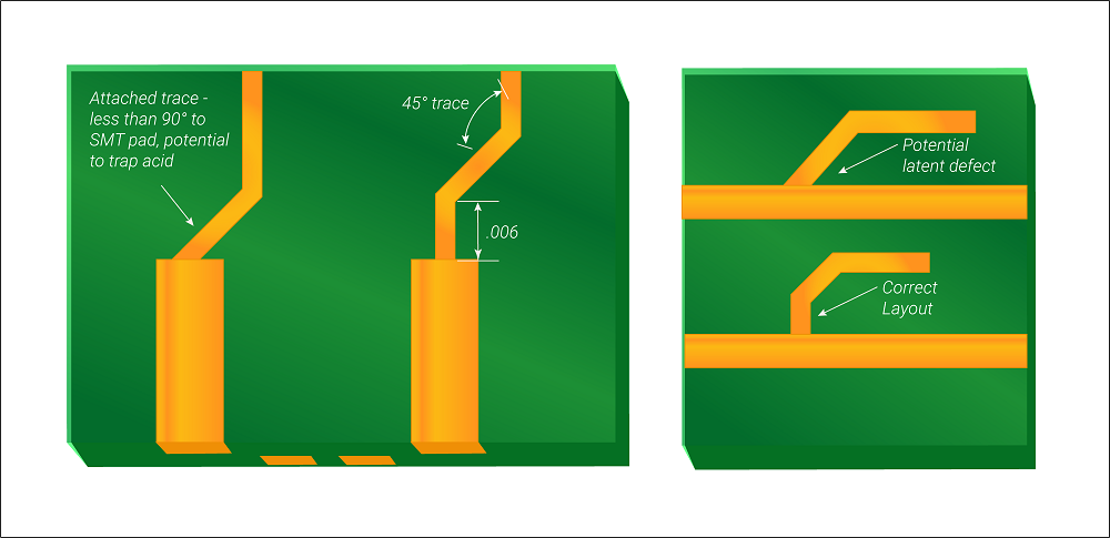
DFM Issues to Check Before PCB Manufacturing

How to use PCB conformal coating ? ultimate guide for beginners - IBE Electronics

How to use PCB conformal coating ? ultimate guide for beginners - IBE Electronics

PCB Etching : a guide to materials, methods, and safety precautions - IBE Electronics

Getting to know PCB terminal blocks : function, material and sizes - IBE Electronics