pcb - Connecting pads with the same functionality belonging to one chip - Electrical Engineering Stack Exchange

I have a question about routing style of pads with the same functionality belonging to one chip. I draw a picture in Paint (fictional IC; let it be the SOIC8 footprint). GND is only as example (it
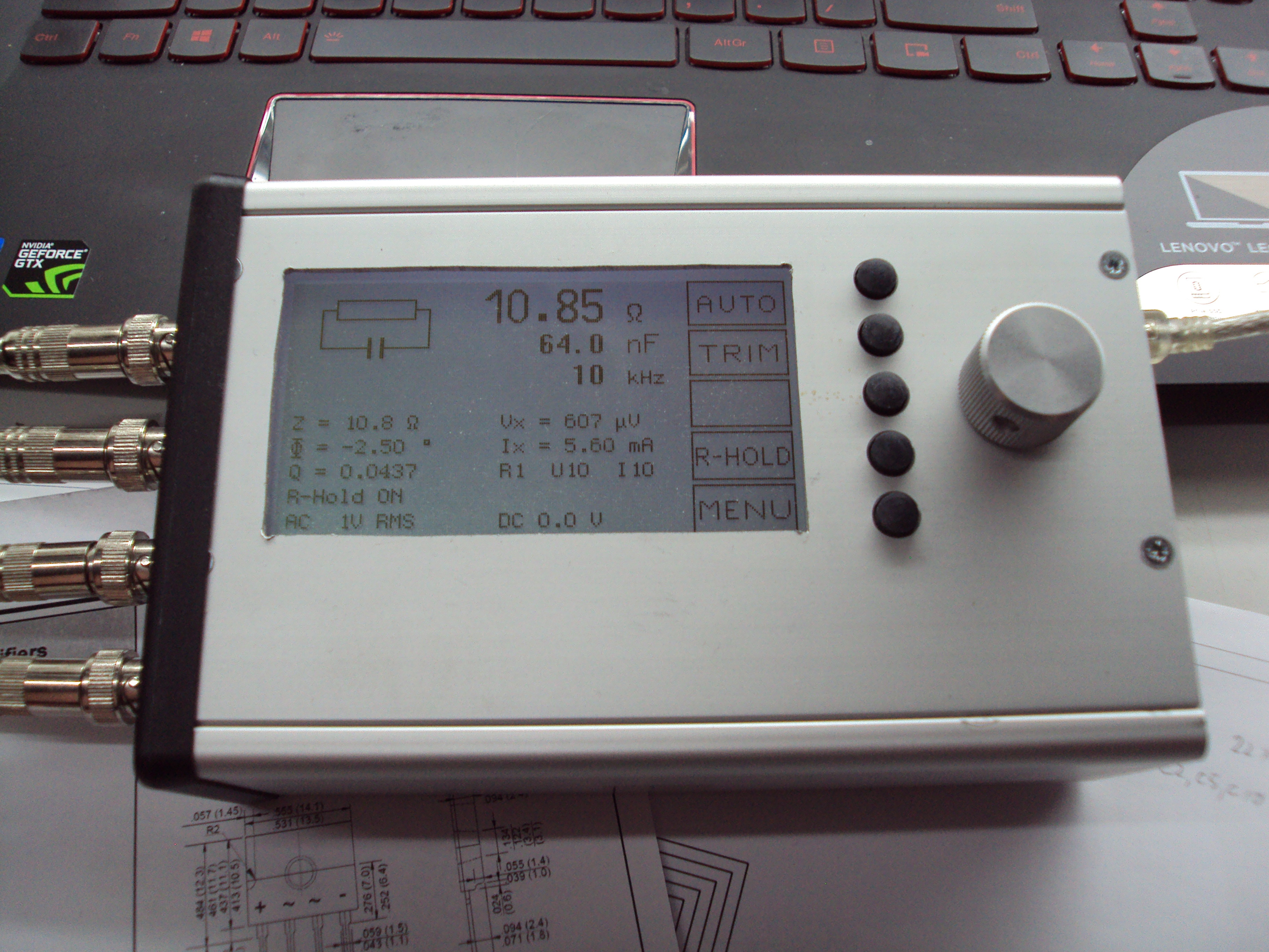
LCR Meter Revisited (AU2019)
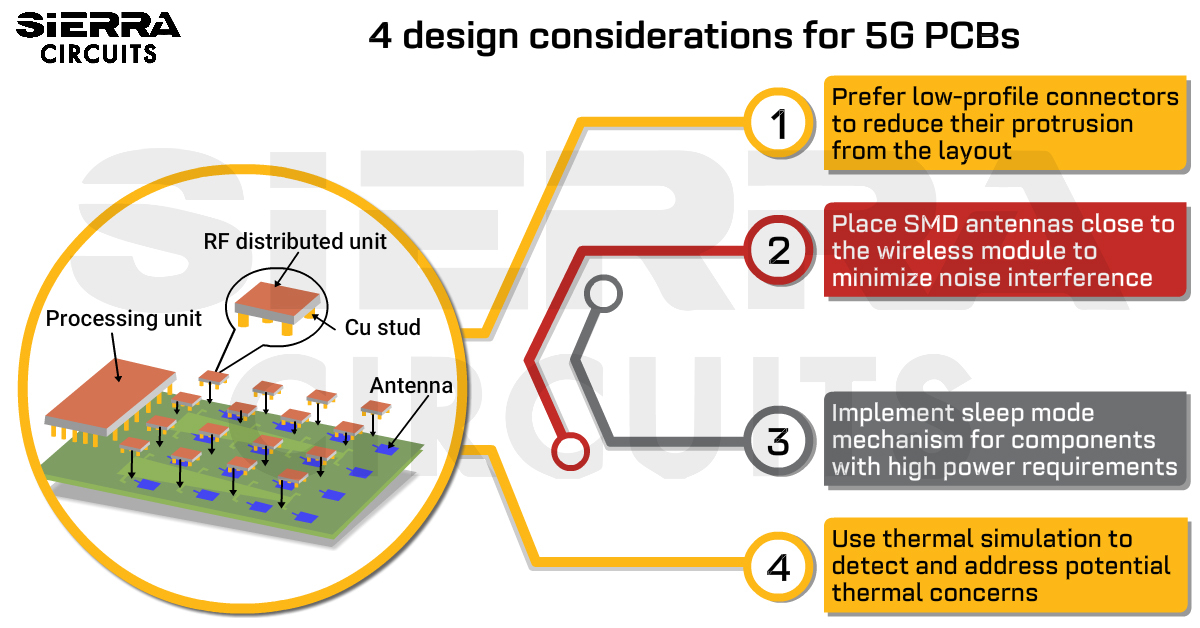
How to Design PCBs for 5G Wireless Applications

pcb - Connecting pads with the same functionality belonging to one chip - Electrical Engineering Stack Exchange
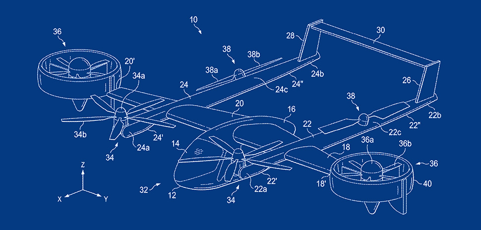
Patented: Textron Innovations' VTOL Aircraft and More North Texas Invetive Activity » Dallas Innovates

Intel 4004 - Wikipedia

Latest News, Events and more from EFFECT Photonics

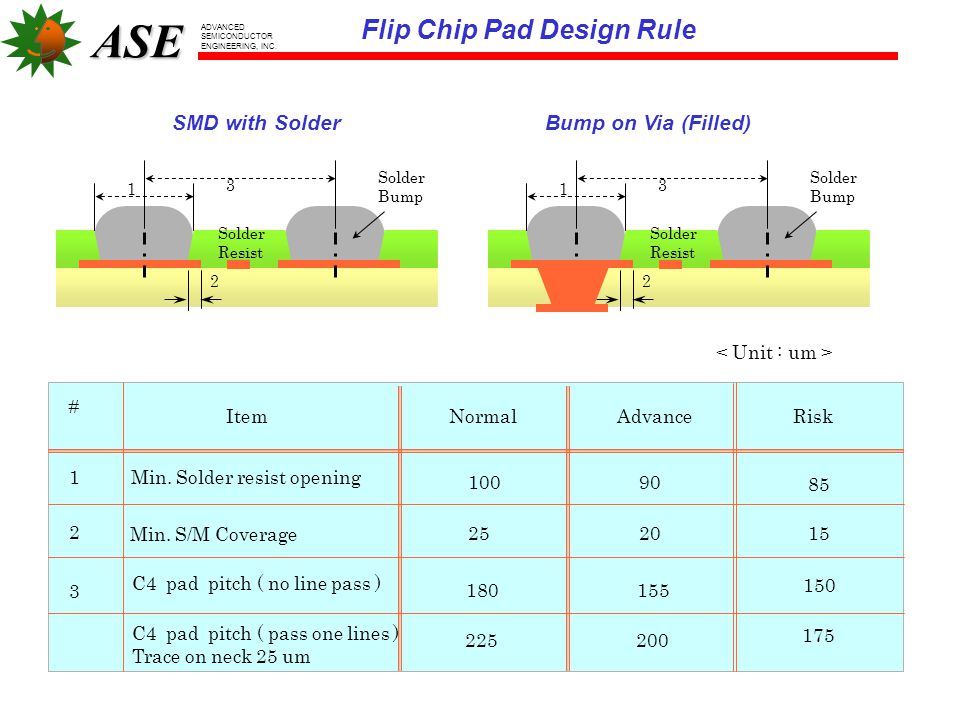
RH108A Datasheet and Product Info

High-Bandwidth Memory (HBM) - Semiconductor Engineering
Selecting the Right Transmission Line Impedance

Unlocking PCB Reverse Engineering: Techniques, Benefits

PCB/Schematic Review - ESP32-S2 Breakout : r/PrintedCircuitBoard


)